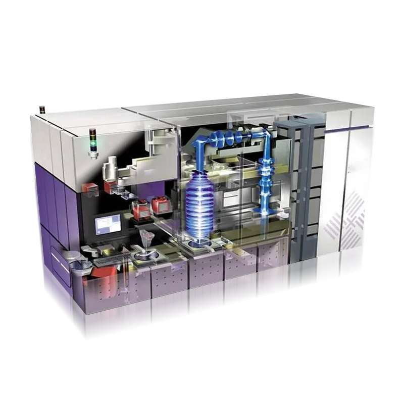
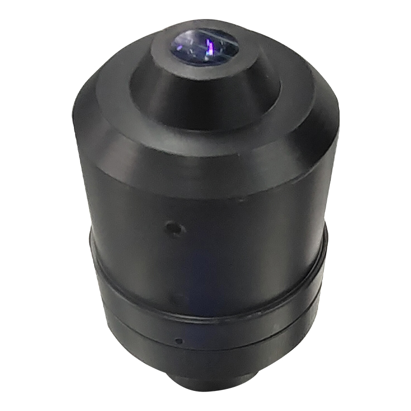
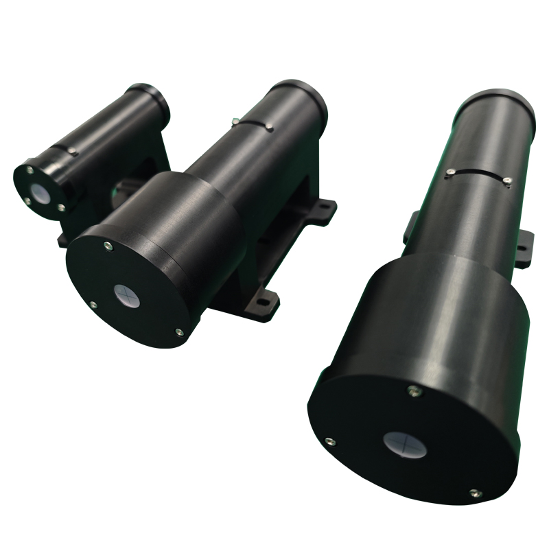
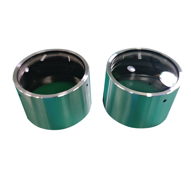
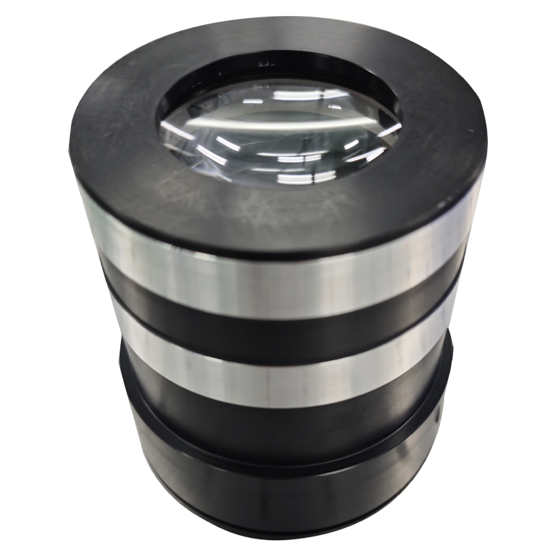
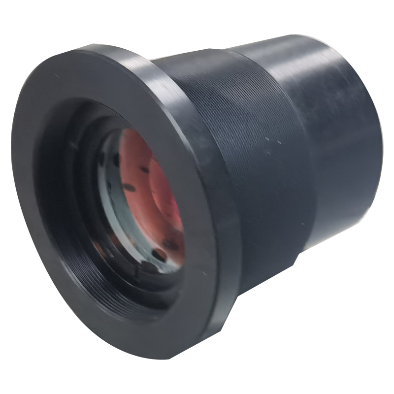
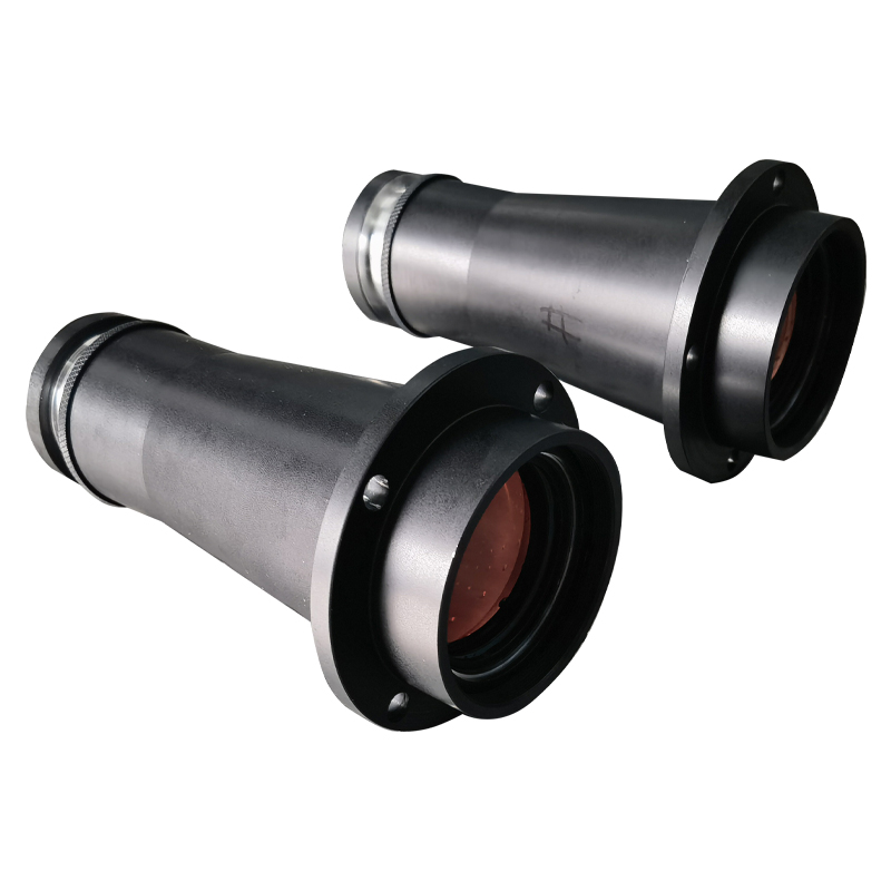
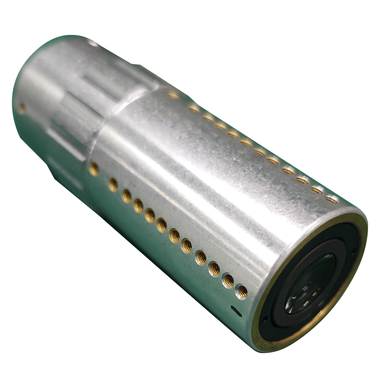
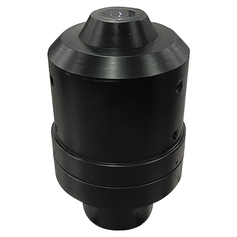
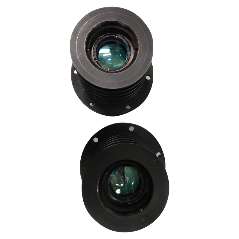
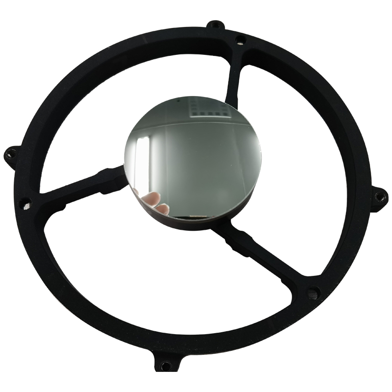
Wafer inspection lens
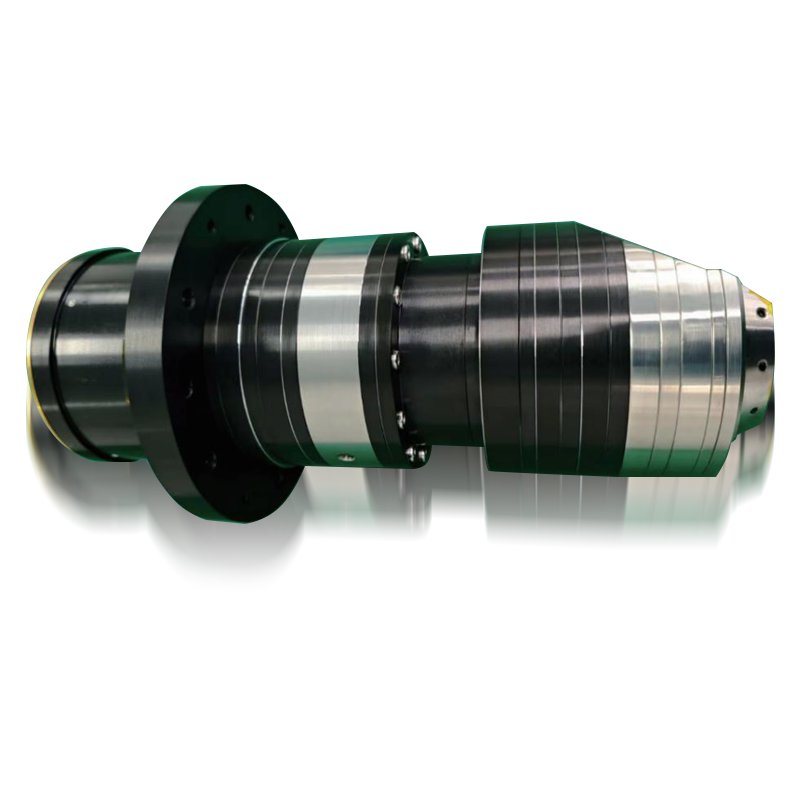
Equipment Accuracy:Through alternating positive and negative focal power combinations, the aberration correction capability of the lithographic projection objective is improved, thereby enhancing exposure imaging quality, achieving smaller exposure resolution and CDU (Critical Dimension Uniformity), and ensuring imaging accuracy and stability.
Detailed Introduction:This lens is one of the core components in semiconductor inspection, composed of multiple optical elements, used to reduce and project the pattern on the photomask onto the silicon wafer in proportion. The design and manufacturing of the lithography machine objective is a complex system engineering involving technologies in optics, mechanics, electronics, software and other fields. On the basis of meeting high exposure resolution, the lens can reduce the number of lenses and aspherical mirrors, lower the design cost and manufacturing cycle of the lithographic projection objective, and enhance the product's market competitiveness.