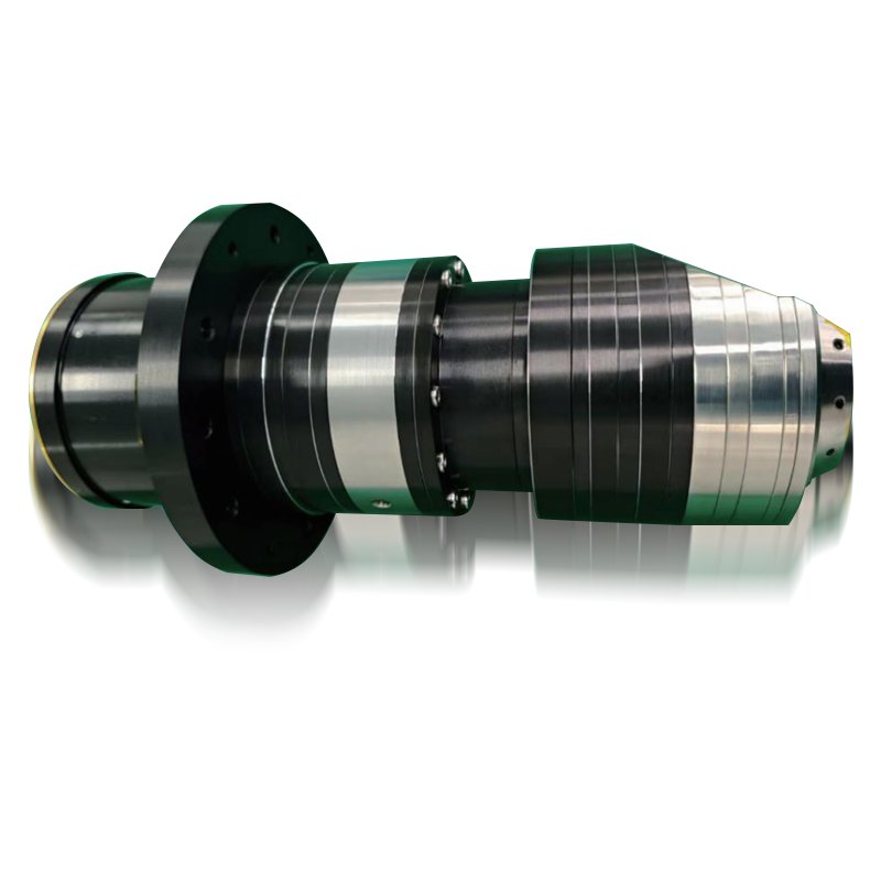
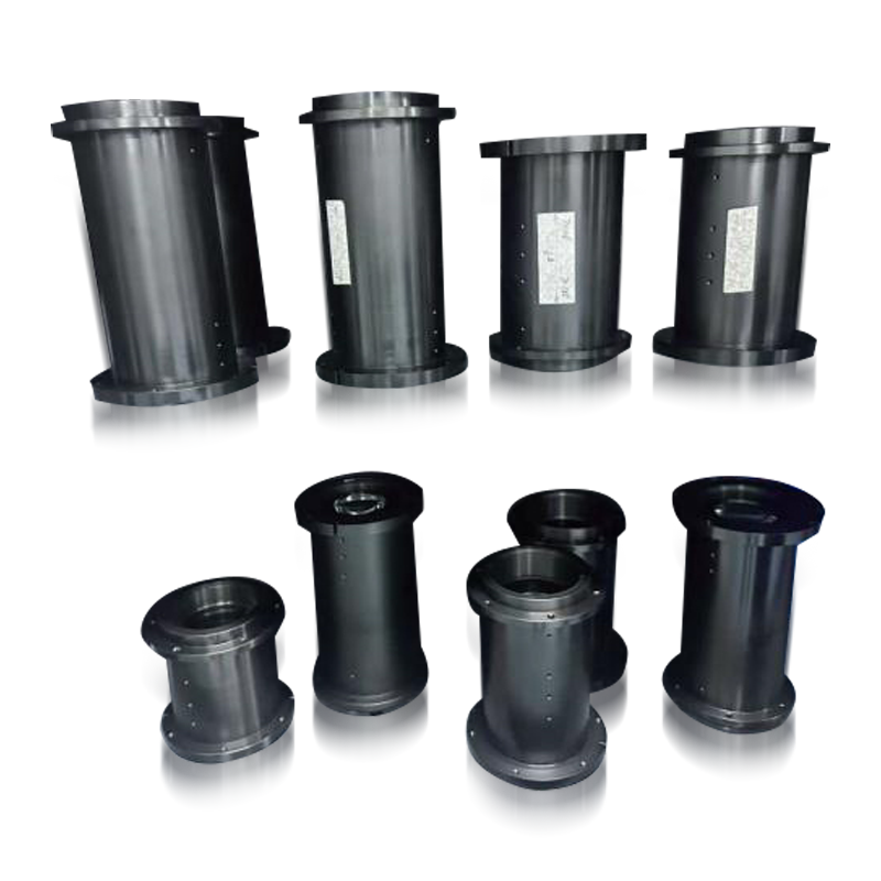
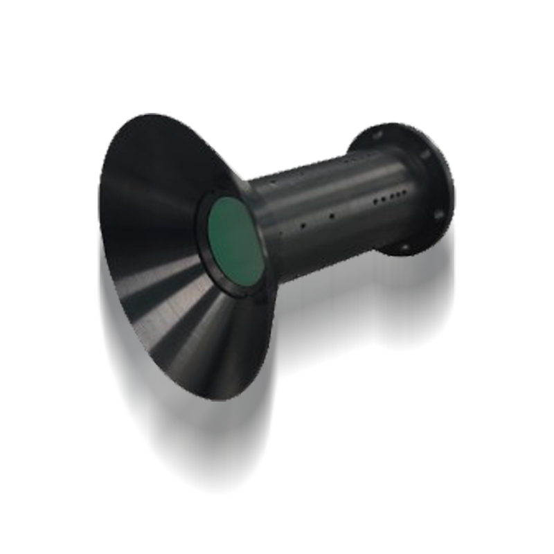
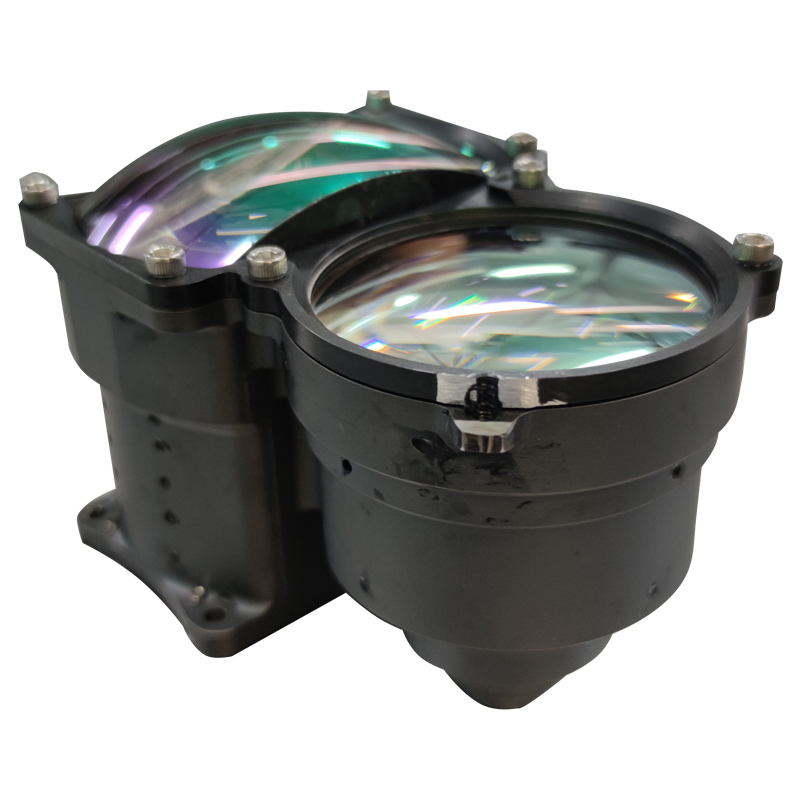
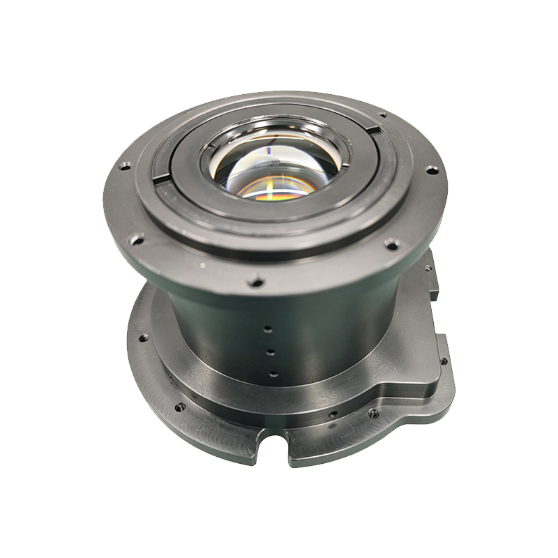
# 266 nm Deep Ultraviolet Objective Lens
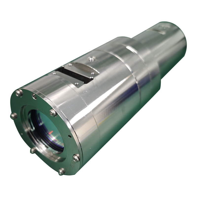
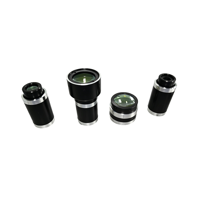
The 266 nm UV objective lens is a high‑precision core optical component custom‑designed for the **266 nm deep ultraviolet (DUV) band** (the fourth harmonic of an Nd:YAG laser). It is primarily suited for deep ultraviolet laser precision machining, high‑end microscopic observation, lithography assistance, and similar applications. With exclusive high resolution, high transmittance, and high laser resistance in the DUV band, it overcomes performance limitations of visible‑light objective lenses and serves as a critical device for precise focusing and clear imaging in deep ultraviolet optical systems.
## I. Core Definition and Band Positioning
266 nm falls within the deep ultraviolet (DUV) band, with a wavelength approximately half that of visible light. Centered at 266 nm, this objective lens also supports 355 nm (near‑UV) auxiliary observation and is optimized for the propagation characteristics and application requirements of deep ultraviolet radiation. Unlike ordinary UV objective lenses, it addresses three key challenges: strong material absorption of DUV light, high difficulty of aberration correction, and high risk of laser damage.
**Optical Type**: Primarily uses an **infinity‑corrected Plan Apochromat (Plan APO)** design. Some versions are specialized for high numerical aperture (HR) or long working distance (LWD) to meet diverse application needs.
**Core Positioning**: Focuses 266 nm DUV laser light to achieve sub‑micrometer machining, or enables high‑resolution observation and inspection of DUV‑sensitive samples (e.g., photoresist, biological fluorescent specimens).
**Key Advantage**: Delivers a resolution improvement of more than 30% compared to 355 nm UV objective lenses, enabling finer micro/nanostructure machining and observation.
---
## II. Key Technical Features
### 1. Optical Design and Aberration Correction
Based on the optical characteristics of the 266 nm DUV band, dedicated apochromatic correction technology is adopted to fully compensate for chromatic aberration, spherical aberration, coma, and field curvature. This ensures sharp imaging and accurate focusing across the entire field of view, free from edge distortion or blurring.
- **High Numerical Aperture (NA)**: NA ranges from 0.5 to 0.8, a core determinant of resolution. At 266 nm and NA = 0.8, theoretical resolution reaches **0.24 μm**, satisfying sub‑micrometer micro/nano machining and observation requirements.
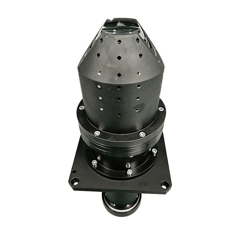
- **Infinity‑Corrected Design**: Compatible with microscope bodies, laser scanning systems, and galvanometer assemblies. It can be flexibly integrated with tube lenses and high‑resolution cameras to achieve integrated “machining + real‑time observation”.
- **Working Distance Compatibility**: Standard WD: 3–12 mm; long‑working‑distance models exceed 50 mm. Suitable for thick samples and machining with protective glass, preventing damage from direct contact between the lens and sample.
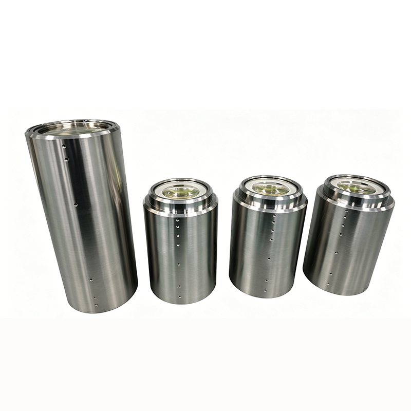
### 2. Material and Coating Technology
Since deep ultraviolet light is easily absorbed by ordinary optical glass, the 266 nm UV objective lens uses specialized materials and coatings to ensure high transmittance and laser durability.
- **DUV High‑Transmission Materials**: Uses **fused silica (SiO₂) or calcium fluoride (CaF₂)** optimized for deep ultraviolet applications, with transmittance ≥ 60% at 266 nm. This effectively reduces optical energy loss and avoids heating and aging caused by UV absorption.
- **Laser‑Resistant Coatings**: Multilayer deep ultraviolet anti‑reflection (AR) coatings optimize transmittance at 266 nm while raising the laser‑induced damage threshold, typically ≥ 0.1 J/cm² (10 ns pulse). This supports high‑power 266 nm pulsed lasers and prevents coating delamination or lens fracture.
- **Non‑Cemented Structure**: High‑end models use air‑spaced non‑cemented lens designs to avoid aging and yellowing of adhesive layers under DUV and high‑power laser exposure, extending service life and improving optical stability.
### 3. Resolution and Imaging Performance
- **Theoretical Resolution**: Based on the Rayleigh criterion, resolution is given by σ = 0.61λ/NA. At 266 nm and NA = 0.8, σ ≈ 0.24 μm, enabling clear observation of sub‑micrometer micro/nanostructures, semiconductor wafer defects, etc.
- **Multi‑Band Compatibility**: Selected models support dual‑band correction for 266 nm (machining) + 355 nm / 532 nm (observation), allowing simultaneous laser machining and real‑time coaxial imaging to improve process accuracy and inspection efficiency.
- **Large Sensor Compatibility**: Supports C‑mount, CS‑mount, and M4/3‑mount interfaces, compatible with 1/2‑inch to 1.2‑inch high‑resolution CMOS/CCD cameras (pixel size ≤ 2 μm) for high‑resolution imaging and inspection.
---
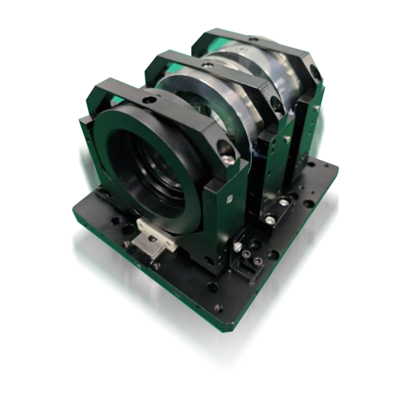
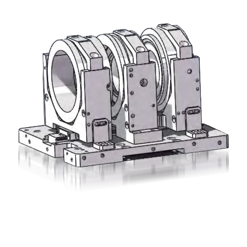
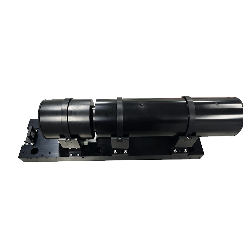
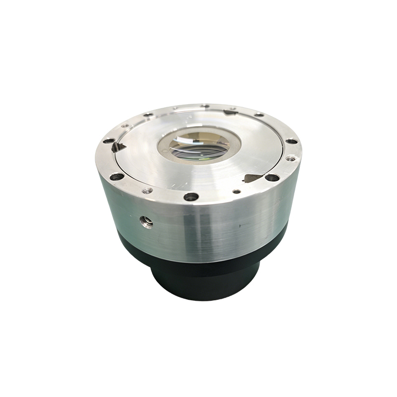
## III. 266 nm UV Objective Lens Compensation System
The 266 nm UV objective lens compensation system is a core supporting assembly tailored to DUV band characteristics that maintains high‑precision lens performance. Its main functions are to compensate for aberrations, thermal effects, and assembly errors introduced during DUV propagation and lens operation. It resolves challenges such as difficult aberration correction, poor thermal stability of materials, and strict assembly tolerances at 266 nm, ensuring sustained sub‑micrometer focusing and imaging accuracy under high‑power lasers, temperature fluctuations, and prolonged operation. It is essential for stable performance in high‑end 266 nm UV objective applications.
### 1. Core Compensation Objectives
Targeting key pain points of 266 nm DUV objectives, the system achieves three core goals covering optical performance, environmental adaptability, and assembly precision to meet strict requirements for DUV precision machining and high‑end observation.
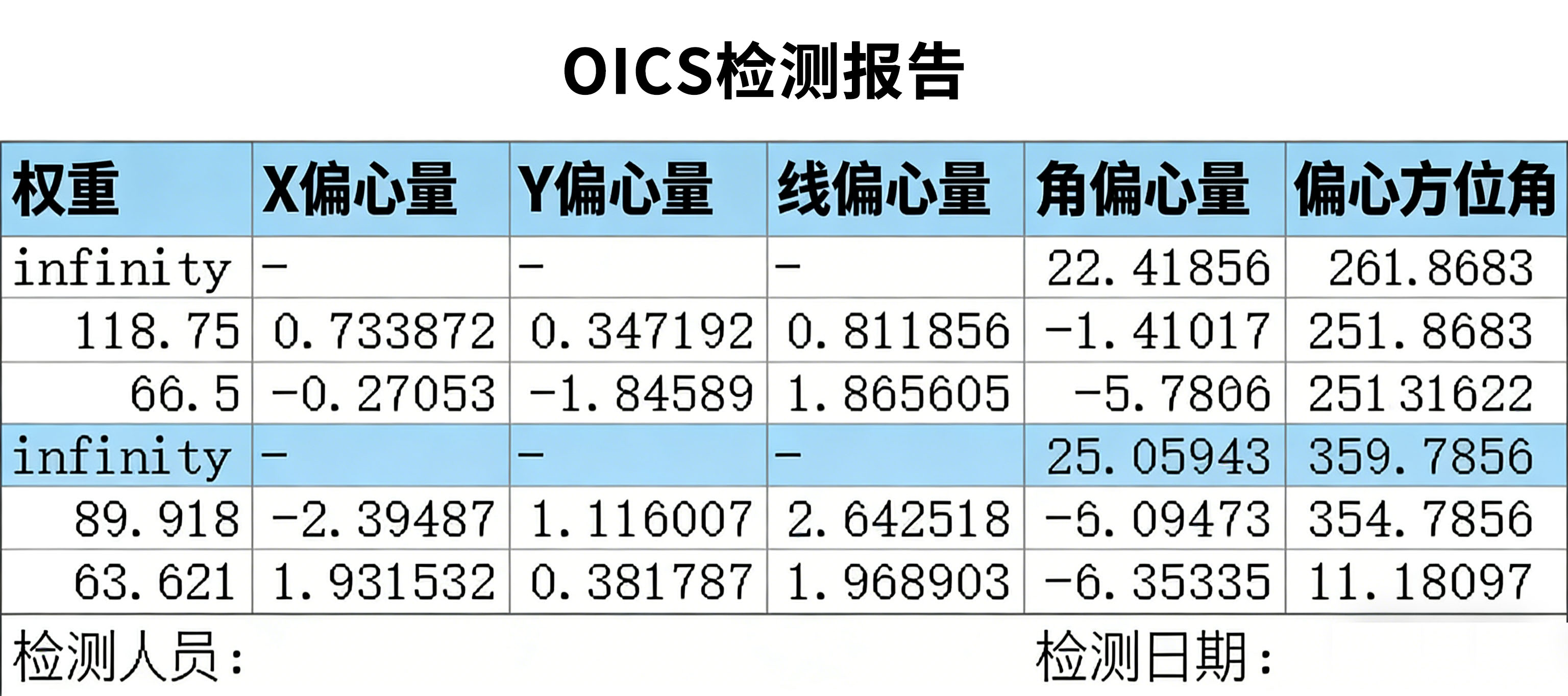
- **Aberration Compensation**: Precisely corrects wavefront aberration, spherical aberration, chromatic aberration, field curvature, and other aberrations. Wavefront error is controlled within 2 nm (suitable for high‑precision lithography), ensuring sharp, distortion‑free imaging across the full field and avoiding reduced machining accuracy and increased observation errors caused by aberrations.
- **Thermal Compensation**: Counteracts defocus caused by thermal expansion/contraction of lens elements, refractive index variations, and barrel deformation due to temperature changes across the operating range of −20 to 60 °C. It especially addresses the poor thermal stability of DUV materials such as calcium fluoride (CaF₂).
- **Assembly and Operating Condition Compensation**: Corrects lens decentration and tilt errors from assembly, performance shifts from heating and minor deformation under high‑power 266 nm laser irradiation, and wavelength shifts in multi‑band applications, ensuring long‑term operational stability.
### 2. Main Compensation Technologies and Implementation
Combining 266 nm DUV characteristics and application scenarios, the system uses optical, mechanical, and electromechanical cooperative compensation, either individually or in combination, balancing precision and engineering practicality.
#### (1) Optical Compensation (Core Foundation)
An integrated, built‑in scheme that achieves aberration and wavelength shift compensation through optical design alone, without external components, suitable for general applications.
- **Apochromatic Compensation**: Uses Plan APO design with fused silica, calcium fluoride, and other specialized materials to precisely compensate chromatic aberration between 266 nm DUV and 355 nm / 532 nm observation light, while correcting spherical aberration and field curvature.
- **Aspherical Lens Compensation**: For high‑resolution objectives with NA ≥ 0.75, aspherical lenses optimize image quality and reduce aberrations without increasing component count, while minimizing lens volume.
- **Reflective Element Compensation**: For ultra‑high‑end objectives with NA ≥ 1.1, catadioptric structures with concave reflective elements effectively correct field curvature and further improve aberration correction for lithography and other ultra‑high‑precision applications.
#### (2) Mechanical Compensation (Environmental Adaptation)
Primarily compensates performance shifts from temperature variations and assembly errors, with simple structure and high reliability, widely used in industrial machining and field inspection.
- **Passive Mechanical Compensation**: Dual‑barrel design with inner lens mount and outer compensation structure. High‑expansion engineering plastic and low‑expansion metal are combined to automatically compensate for image shift due to temperature, achieving athermal design from −20 to 60 °C with system MTF > 0.4.
- **Assembly Error Compensation**: Precision mechanical structures constrain lens decentration and spacing. Rear group decentration is controlled within 0.005 mm, and thickness tolerance of dual‑separated lenses within 0.005 mm, reducing assembly‑induced aberrations and improving consistency.
#### (3) Electromechanical Cooperative Compensation (High‑End Precision)
For ultra‑high‑precision applications such as lithography and advanced research, an “optical + mechanical + electronic control” scheme enables dynamic real‑time compensation, restoring thermal and wavefront aberrations near design levels.
- **Movable Lens Compensation**: Internally integrated movable lens groups, electrically driven for vertical and tilt adjustment to dynamically eliminate aberrations from assembly and operation, especially under high‑power laser deformation.
- **Element Displacement and Zoned Heating Cooperative Compensation**: Electrically adjusts lens spacing, decentration, or tilt. By exploiting temperature‑dependent refractive index changes, zoned heating generates a controlled wavefront, reducing wavefront error from 129.78 nm to 1.69 nm and distortion from 12.24 nm to 1.31 nm.
- **Precision Temperature Control**: Multi‑stage external heat flux suppression and indirect radiation control maintain temperature stability of lenses and CMOS/CCD detectors within ±0.3 °C, minimizing thermal drift for long‑term accuracy.
### 3. Key Parameters and Application Scenarios
| Compensation Type | Key Parameters | Typical Applications |
|--------------------|----------------|----------------------|
| Optical Compensation | Wavefront error ≤ 2 nm; chromatic correction 266–532 nm | General precision machining, basic microscopy |
| Mechanical Compensation | Temperature range −20~60 °C; MTF ≥ 0.4 | Industrial in‑line machining, field inspection |
| Electromechanical Compensation | Temperature stability ±0.3 °C; wavefront error ≤ 1.7 nm | Lithography, advanced research, sub‑micrometer inspection |
### 4. Operation and Maintenance Guidelines
- **Parameter Matching**: Select compensation type according to lens model (high‑resolution / long working distance) and application (machining / observation). Electromechanical compensation is preferred for high‑NA and high‑precision scenarios; mechanical thermal compensation for large temperature variations.
- **Regular Calibration**: Calibrate movable lens positioning and temperature control every 3–6 months for electromechanical systems. Inspect dual‑barrel fit for mechanical systems to avoid dust or oil contamination.
- **Environmental Control**: Avoid operation under extreme temperature swings (outside −20~60 °C) or high humidity to prevent structural deformation and lens fogging. Use cooling systems under high‑power laser conditions to reduce thermal load.
- **Assembly Care**: Avoid touching compensation components (movable lenses, compensation barrels) during disassembly and cleaning. Follow strict tolerance specifications to maintain required lens decentration and spacing.