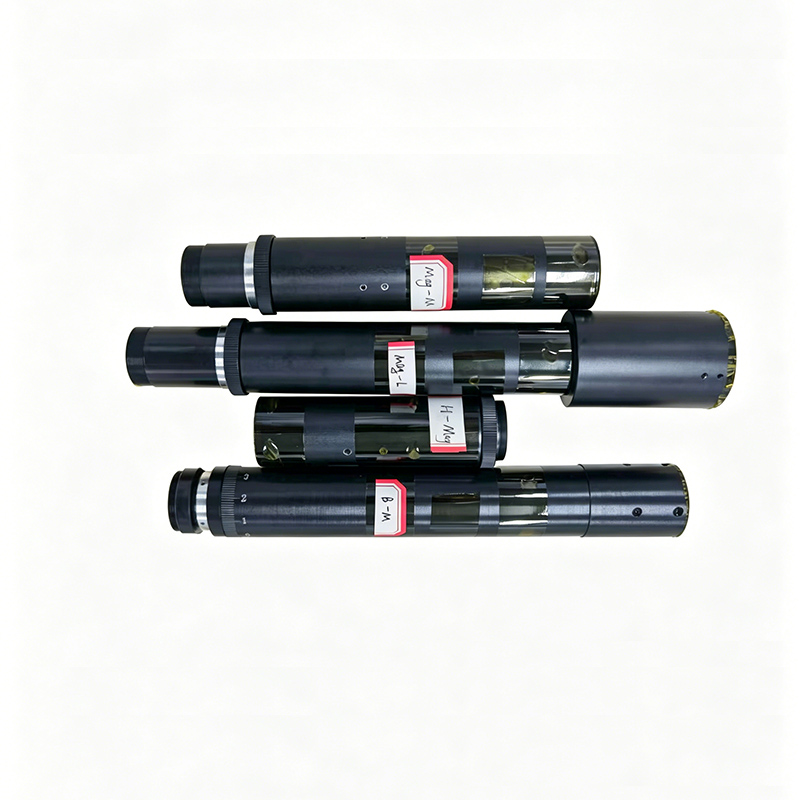
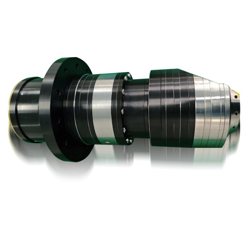
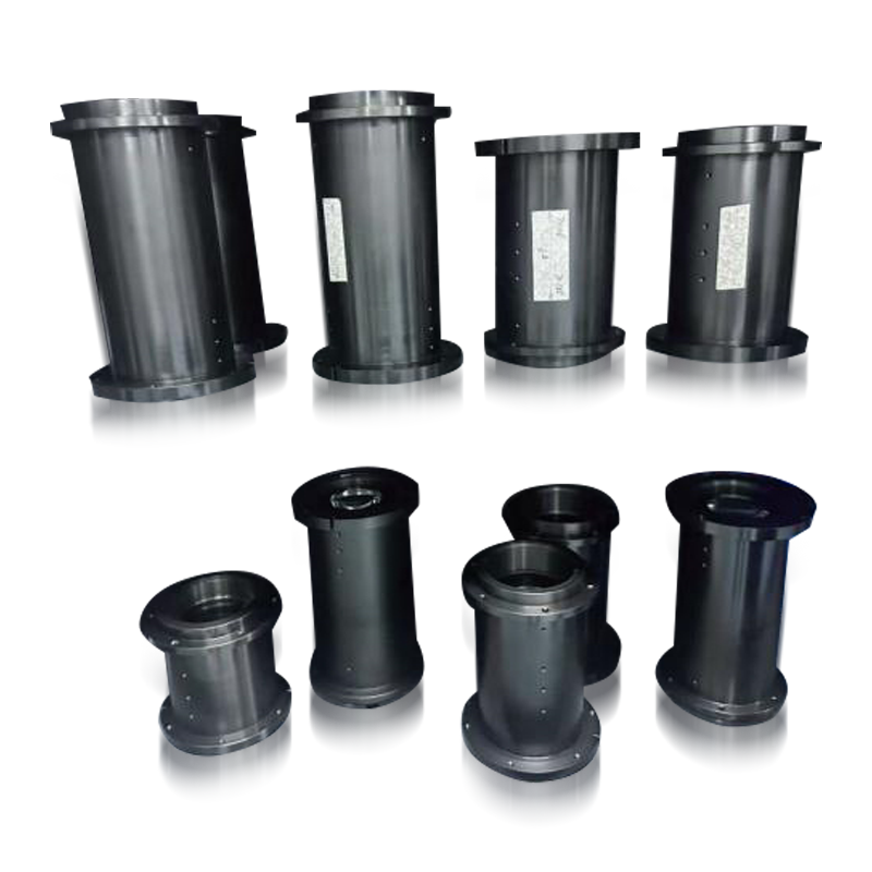
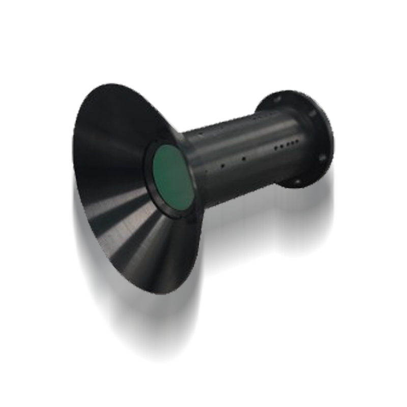
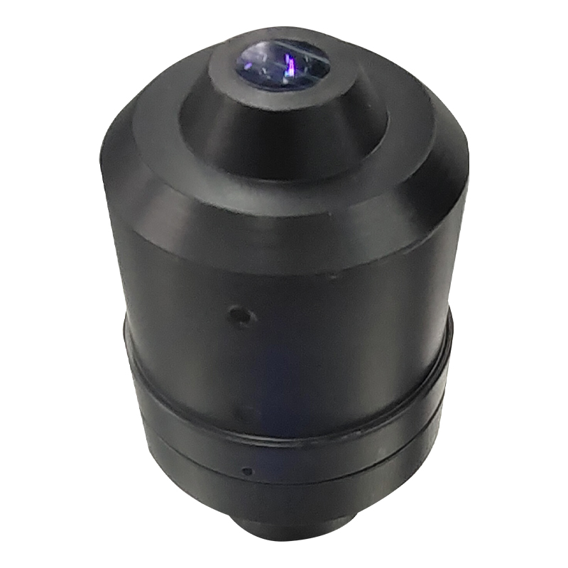
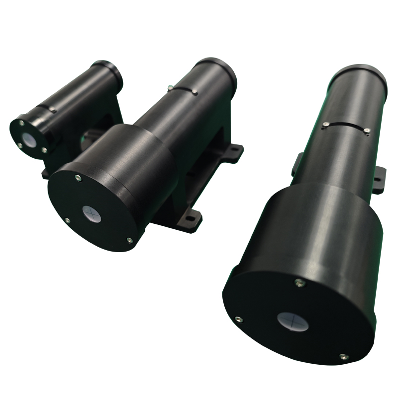
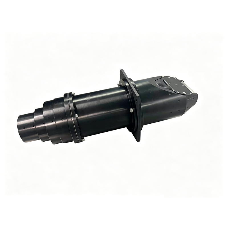
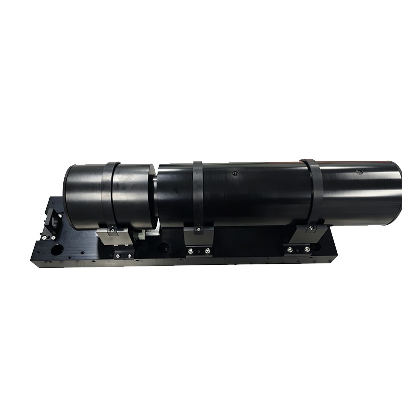
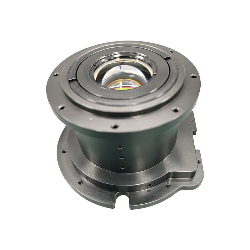
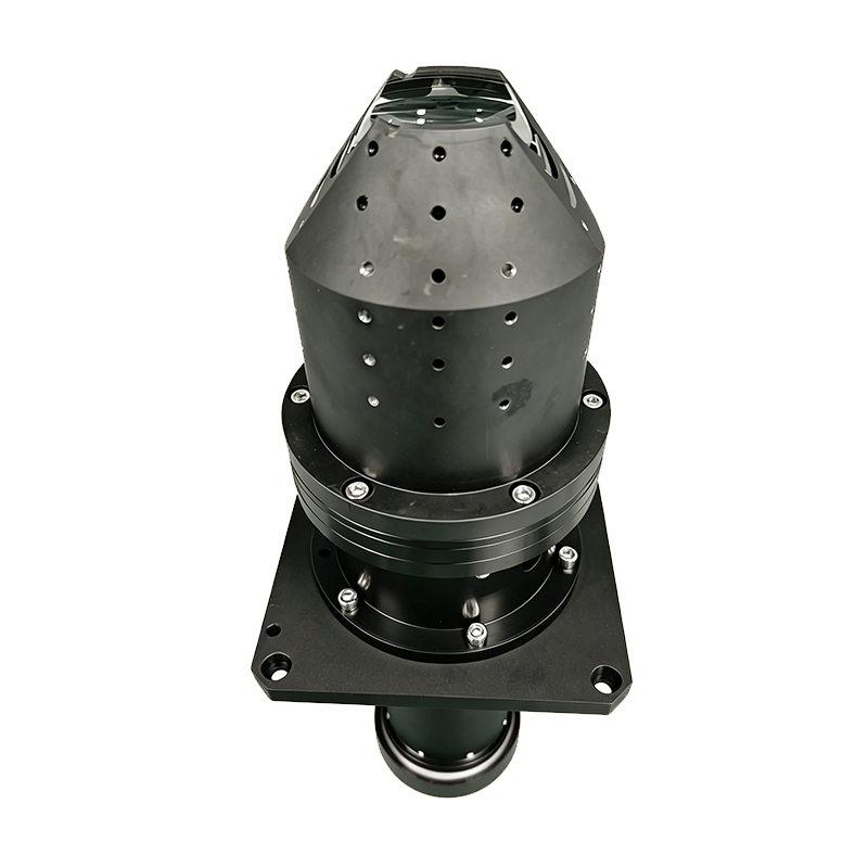
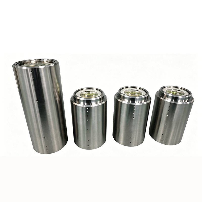
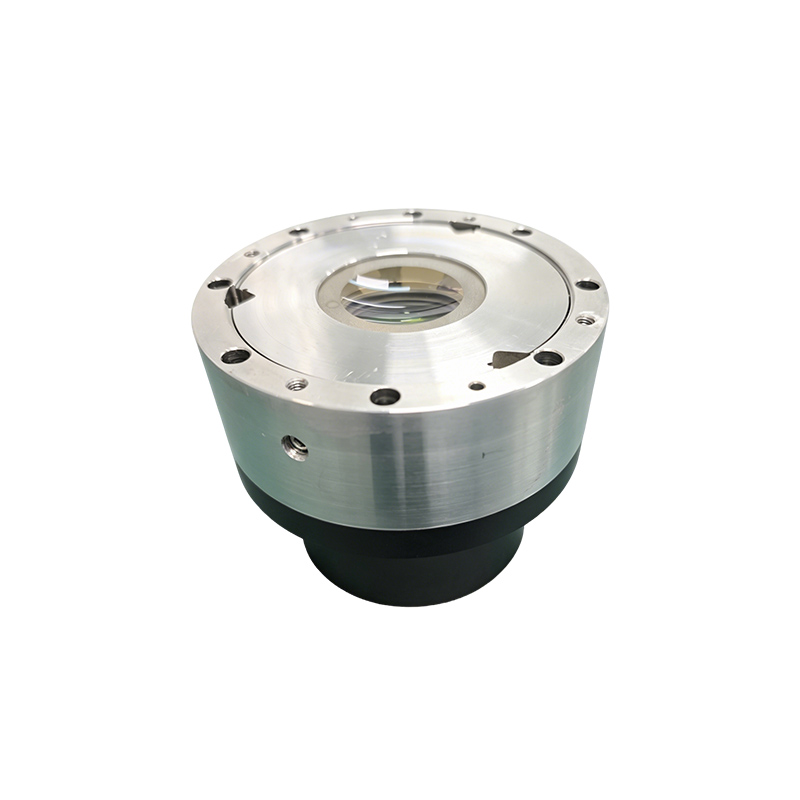
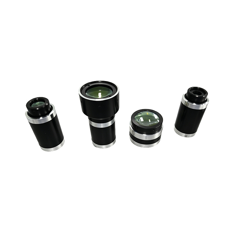
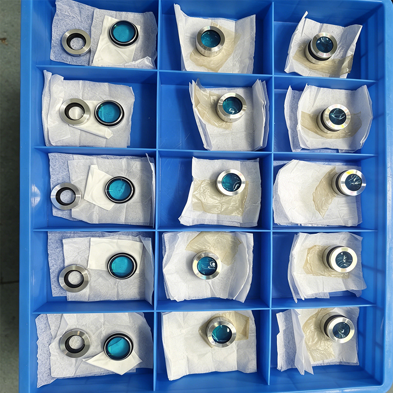
Bright & Dark Field Inspection Lens for Wafers
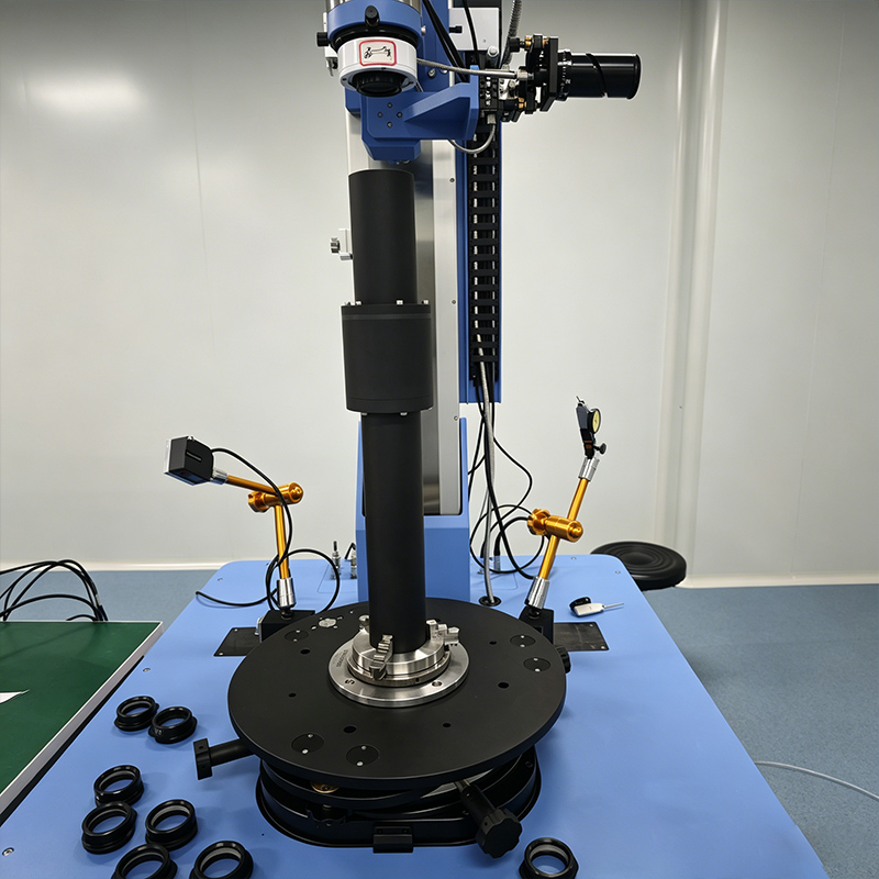
Equipment Accuracy:
Detailed Introduction:This wafer bright/dark field objective is an infinity-corrected plan compound objective specially developed for semiconductor wafer defect inspection. A single objective integrates dual bright-field and dark-field optical paths. It is compatible with metallographic microscopes, semiconductor inspection microscopes and wafer AOI equipment. It is applied to defect detection of 6/8/12-inch bare wafers, post-photolithography wafers and diced chips, and acts as a core optical component for semiconductor front-end processes and packaging quality inspection.